TN State Board 12th Physics Important Questions Chapter 9 Semiconductor Electronics
Question 1.
In a photo diode, the conductivity increases when the material is exposed to light, It is found that conductivity charges only if the wavelength is less than 620 nm. What is the band gap?
Answer:
Question 2.
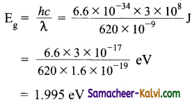
An alloy semiconductor gallium arsenide phosphide is 1.98 eV. Calculate the wavelength of radiation that is emitted when electrons and holes in this material combine directly. What is the colour of the emitted radiation?
Answer:
Wave length λ = \(\frac{h c}{\mathrm{E}_{g}}=\frac{6.6 \times 10^{-34} \times 3 \times 10^{8}}{1.98 \times 1.6 \times 10^{-19}}\)
= 6.25 × 10-7 = 6250 Å
The colour of emitted radiation is red.
![]()
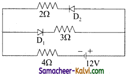
Question 3.
The circuit has two oppositely connected ideal diodes in parallel. What is the current flowing in the circuit?
Answer:
Since diode D1 is reverse biased, no current flows through it. Only diode D2 conduct because it is forward biased
I = \(\frac{V}{R}=\frac{12}{2+4}\) = 2 A
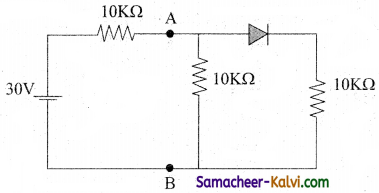
Question 4.
In the given circuit, the potential difference between A and 8 is;
Answer:
The forward biased p-n junction does not offer any resistance.
∴ RAB = \(\frac{10 \times 10}{10+10}\)
= 5 KΩ
Total resistance, R = 10 + 5 = 15KΩ
Current in the circuit,
I = \(\frac{V}{R}=\frac{30 V}{15 \times 10^{3}}\)
= 2 × 10⁻³ A
Current through each arm = \(\frac{I}{2}\) = 10-3 A
∴ Potential difference between A and B is VAB = 10 × 10 + 3 × 10-3 = 10 V
![]()
Question 5.
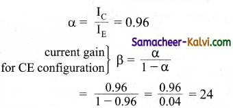
The current gain of a transistor \(\frac{\mathrm{I}_{\mathrm{C}}}{\mathrm{I}_{\mathrm{E}}}=\) = 0.96 then, what is the current gain for CE configuration?
Answer:
For CE configuration, the current transfer ratio is
Question 6.
Distinguish between n-type and p-type semiconductors.
Answer:
| n – type semiconductor | p – type semiconductor |
| These are extrinsic semiconductor obtained by doping impurity atoms of group V to Ge or Si crystal. | These are extrinsic semiconductor obtained by doping impurity atoms of group III to Ge or Si crystals. |
| The impurity atoms added provide free electrons and one called donors. | The impurity atoms added create vacancies of electrons (or holes) and are called acceptors. |
| The donor impurity level lies just below the conduction band. | The acceptor impurity level lies just above the valence band. |
| The electrons are majority charge carriers while holes are minority charge carriers. | The holes are majority charge carriers while electrons are minority charge carrier. |
| The free electron density is much greater than hole density, i.e., ne >> nn | The hole density is much greater than free electron density. ; i.e., nn >> ne |
![]()
Question 7.
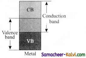
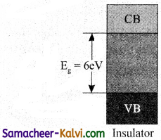
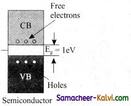
Distinguish between metals, insulators and semiconductors on the basis of band theory.
Answer:
Depending upon energy band gap is zero, large or small, the solids may be classified into metals, insulators and semiconductors as explained below.
(i) Metals:
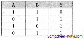
The energy band structure of metal as shown in figure. The valence band and the conduction band are overlap with each other. Hence, electrons can move freely into the conduction band which results in a large number of free electrons in the conduction band.
Therefore, conduction becomes possible even at low temperature. The application of electric field provides sufficient energy to the electrons to drift in a particular direction to constitute a current. For metals the resistivity value lies between 10-2 and 10-8 Ωm.
Insulators:
The energy band structure of insulators is shown in figure. The valence band and the conduction band are separated by a large energy gap. The forbidden energy gap is approximately 6 eV in insulators. The energy gap is very large that electrons from valence band cannot move into conduction band even on the application of strong external electric field or the increase in temperature. Therefore, the electrical conduction is not possible as the free electrons are almost nil and hence these materials are called insulators. Its resistivity is in the range of 1011 to 1019 Ωm.
(iii) Semi conductors:
In semiconductors, there exists a narrow forbidden energy gap (Eg < 3 eV) between the valence band and the conduction band. At a finite temperature, thermal agitations in the solid can break the covalent bond between the atoms. This releases some electrons from valence band to the conduction band.
Since free electrons are small in number, the conductivity of the semiconductors is not as high m that of the conductors. The resistivity value of semiconductors is from 105 to 106 Ωm. When the temperature is increased further, more number of electrons is promoted to the conduction band and increases the conduction.
Thus, we can say that the electrical conduction increases with the increase in temperature. In other words, resistance decreases with increase in temperature. Hence, semiconductors are said to have negative temperature 1 coefficient of resistance. The forbidden energy gap for Si and Ge at room temperature are 1.1 eV and 0.7 eV respectively.
![]()
Question 8.
Sketch and explain the energy band diagram of intrinsic and extrinsic semiconductors.
Answer:
(i) Energy band diagram of intrinsic semiconductor:
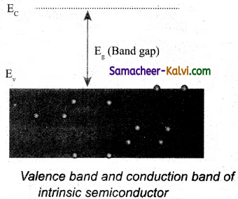
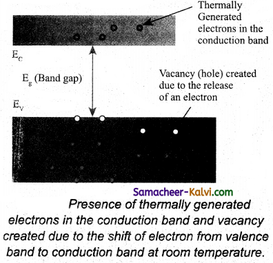
At T = 0 K, the valence band of a semiconductor is completely filled with electrons while the conduction band is empty as shown in fig (a). Hence an intrinsic semiconductor behaves like an insulator at T = 0 K. At higher temperature (T > 0 K), some electrons of the valence band gain sufficient thermal energy and jump to the conduction band, creating an equal number of holes in the valence band.
These thermally excited electrons occupy the lowest possible energy levels in the conduction band. Therefore, the energy band diagram of an intrinsic semiconductor at T > 0 K is of the type shown in figure (b). Clearly, the number of electrons in the conduction band is equal to the number of holes in valence band.
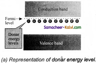
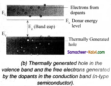
(ii) Energy band diagram of n-type semiconductors:
In n-type semiconduc-tors, extra (fifth) electron is very weakly attracted by the donor impurity. A very small energy (≈ 0.01 eV) is required to free this electron from donor impurity. When freed, this electron will occupy the lowest possible energy level in the conduction band i.e., the energy of the donor electron -is slightly less than E .
Thus the donor energy level ED lies just below the bottom of the conduction band as shown in figure. At room temperature this small energy gap is easily covered by the thermally excited electrons. The conduction band has more electrons (than holes in valence band) as they have been contributed both by thermal excitation and donor impurities.
(iii) Energy band diagram of p – type semi conductors:
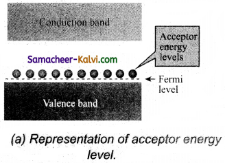
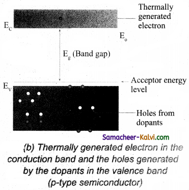
In p – type semiconductors, each acceptor impurity creates a hole which can be easily filled by an electron of Si – Si covalent bond. A very small energy is required by an electron of the valence band to move into this hole. Hence the
acceptor energy EA lies slightly above the top of the valence band.
At room temperature, many electrons of the valence band get excited to these acceptor energy levels, leaving behind equal number of holes in the valence band. These holes can conduct current. Thus the valence band has more holes than electrons in the conduction band.
![]()
Question 9.
What is a BJT? Mention its two types. Give their symbolic representations. Describe the construction of BJT and state the function of its each parts.
Answer:
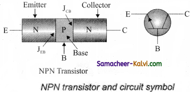
The bipolar junction transistor (BJT) is a three terminal solid state device obtained by growing either a narrow section of p – type crystal between two relatively thicker sections of n – type crystals or a narrow section of n – type crystal between two thicker sections ofp – type crystals.
Transistors are of two types:
(i) NFN transistor:
It consists of a thin section of p – type semiconductor sandwiched between two thicker sections of n – type semiconductor. Figure shows the NPN transistor and its circuit symbol. The arrow head in the symbol points outwards.
(ii) PNP transistor:
It consists of a thin section of n – type semiconductor sandwiched between two thicker sections of p – type semiconductors. Fig shows the PNP transistor and its circuit symbol. The arrow head in the symbol points inwards.
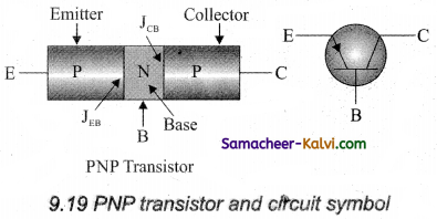
In both types of transistors, the arrow head on the emitter points in the direction of conventional current. Each type of transistor has three main parts:
(i) Emitter (E):
It is a section on one side of the transistor. It is of moderate size and heavily doped semiconductor. It is normally forward biased with respect to any other part of the transistor. It supplies a large number of majority charge carriers for the flow of current through the transistor.
(ii) Base (B):
It is the middle section. It is very thin and lightly doped. It controls the flow of majority charge carriers from emitter to collector.
(iii) Collector (C):
It is section on the other side of the transistor. It is moderately doped and larger in size as compared to the emitter. It is normally reverse biased with respect to any other part of the transistor. It collects the majority charge carriers for the circuit operations.
![]()
Question 10.
Draw the three types of circuit arrangements in which an NPN transistor can be used.
Answer:
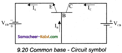
A transistor is a three element device. One terminal has to be always common to the input and the output circuits. This terminal is connected to the ground and serves as a reference point for the entire circuit. So a transistor can be used in one of the following three configurations.
(i) Common-base configuration:
The base is common to both the input and output circuits as shown in figure. The input current is the emitter current IE and the output current is the collector current IC. The input signal is applied between emitter and base, the output is measured between collector and base.
(ii) Common-Emitter configuration:
In this configuration, the emitter is common to both the input and output loops as shown in figure. Base current IB is the input current and the collector current IC is the output current. The input signal is applied between the emitter and base and the output is measured between the collector and the emitter.
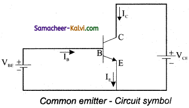
(iii) Common-collector configuration: Here, the collector is common to both the input and output circuits as shown in figure. The base current IB is the input current, the emitter current IF is the output current. The input signal is applied between the base and the collector, the output is measured between the emitter and collector.
Question 11.
Define the two current gains of a transistor and deduce a relation between them.
Answer:
Two types of current gains are defined for a transistor.
(i) Common base current amplification factor (or) AC current gain (α).
It is defined as the ratio of the small change in the collector current to the small change in the emitter current when the collector-base voltage is kept constant.
Thus α = \(\left(\frac{\Delta I_{C}}{\Delta I_{E}}\right)\)
VCB = constant
(ii) Common emitter current amplification factor (or) AC current gain (β):
It is defined as the ratio of the small change in the collector current to the small change in the base current when the collector – emitter voltage is kept constant.
β = \(\left(\frac{\Delta \mathrm{I}_{\mathrm{C}}}{\Delta \mathrm{I}_{\mathrm{B}}}\right)\)
VCE = constant
Relation between α and β:
For both NPN and PNP transistors, we have IE = IB + IC
For small changes, we can write
∆IE = ∆IB + ∆IC
Dividing both sides by ∆IC
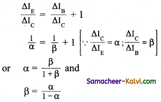
![]()
Multiple Choice Questions:
Question 1.
The cause of potential barrier in a p-n junction diode is:
(a) depletion of positive charges near the junction.
(b) concentration of positive charges near the junction.
(c) depletion of negative charges near the junction.
(d) concentration of positive and negative charges near the junction.
Answer:
(d) concentration of positive and negative charges near the junction.
Question 2.
A semiconductor device is connected in series in circuit with a battery and resistance. A current is allowed to pass through the circuit. If the polarity of the battery is reversed, the current drops to almost zero. The device may be:
(a) a p-n junction diode
(b) an intrinsic semiconductor
(c) a n-type semiconductor
(d) an p-type semiconductor
Answer:
(a) a p-n junction diode
Question 3.
Which of the following when added as an impurity into silicon produces 72-type semiconductor?
(a) P
(b) Al
(c) B
(d) Mg
Answer:
(a) P
![]()
Question 4.
In a junction diode, the holes are due to:
(a) protons
(b) extra electrons
(c) neutrons
(d) missing electrons
Answer:
(d) missing electrons
Question 5.
Depletion layer consists of:
(a) electron
(b) protons
(c) mobile charge carriers
(d) immobile ions
Answer:
(d) immobile ions
Question 6.
In p-type semiconductor, the majority charge carriers are:
(a) protons
(b) holes
(c) electrons
(d) neutrons
Answer:
(b) holes
![]()
Question 7.
In forward bias the width of the depletion layer in a p-n junction diode:
(a) increases
(b) remain constant
(c) decreases
(d) first increases then decreases
Answer:
(c) decreases
Question 8.
Reverse bias applied to a junction diode:
(a) lowers the potential barrier
(b) raises the potential barrier
(c) increases the majority carrier current
(d) increases the minority carrier current
Answer:
(b) raises the potential barrier
Question 9.
Barrier potential of a p-n junction diode does not depend on:
(a) diode design
(b) temperature
(c) forward bias
(d) doping density
Answer:
(a) diode design
![]()
Question 10.
In p – n junction:
(a) high potential is at n-side and low potential at p-side
(b) high potential is at p-side and low potential at n-side
(c) p and n both are at same potential
(d) undetermined
Answer:
(a) high potential is at n-side and low potential at p-side.
Question 11.
Si and Cu are cooled to a temperature of 300 K, then resistivity:
(a) for Si increases and for Cu decreases
(b) for Cu increases and for Si decreases
(c) decreases for both Si and Cu
(d) increases for both Si and Cu
Answer:
(a) for Si increases and for Cu decreases
Question 12.
A n-p-n transistor conducts when:
(a) both collector and emitter are positive with respect to the base.
(b) collector is positive and emitter is at same potential as the base.
(c) collector is positive and emitter is negative with respect to the base.
(d) both collector
Answer:
(c) collector is positive and emitter is negative with respect to the base.
![]()
Question 13.
In semiconductors at room temperature:
(a) the valence band is completely filled and the conduction band is partially filled.
(b) the valence band is completely filled.
(c) the conduction band is completely empty.
(d) the valence band is partially empty and the conduction band is partially filled
Answer:
(d) the valence band is partially empty and the conduction band is partially filled
Question 14.
Zener diode is used for:
(a) rectification
(b) stabilization
(c) amplification
(d) producing oscillations in an oscillators
Answer:
(b) stabilization
Question 15.
Carbon, silicon and germanium atoms have four valence electron each. Their valence and conduction bands are separated by energy band gaps represented by (Eg)C, (Eg)Si and (Eg)Ge respectively. Which one of the following relationship is true in their case.
(a) (Eg)C < (Eg)Ge
(b) (Eg)C > (Eg)Si
(c) (Eg)C = (Eg)Si
(d) (Eg)C < (Eg)Si
Answer:
(b) (Eg)C > (Eg)Si
![]()
Question 16.
Application of a forward bias to a p-n junction:
(a) widens the depletion zone
(b) increases the number of donors on the n-side.
(c) increases the potential difference across the depletion zone.
(d) increases the electric field in the depletion zone.
Answer:
(d) increases the electric field in the depletion zone.
Question 17.
The device that can act as a complete electronic circuit is:
(a) Zener diode
(b) junction diode
(c) integrated circuits
(d) junction transistor
Answer:
(c) integrated circuits
Question 18.
Which of the following statement is false?
(a) The resistance of intrinsic semiconductor decreases with increase of temperature
(b) Pure Si doped with trivalent impurity gives a p-type semiconductor.
(c) Majority carriers in a n-type semi conductors are holes.
(d) Minority carriers in a p-type semi conductor are electrons.
Answer:
(c) Majority carriers in a n-type semi conductors are holes.
![]()
Question 19.
Choose the only false statement from the following:
(a) The resistivity of a semiconductor increases with increase in temperature.
(b) Substances with an energy gap of the order of 10 eV are insulators.
(c) In conductors, the valence and conduction bands may overlap.
(d) The conductivity of a semiconductor increases with increase in temperature.
Answer:
(a) The resistivity of a semiconductor increases with increase in temperature.
Question 20.
If a small amount of antimony is added to germanium crystal:
(a) there will be more free electrons from hole in the semiconductor.
(b) its resistance is increased.
(c) it become a p-type semiconductor
(d) the antimony becomes an acceptor atom
Answer:
(a) there will be more free electrons from hole in the semiconductor.
Question 21.
A photocell employs photo electric effect to convert:
(a) change in the intensity of illumination into a change in photoelectric current.
(b) change in the frequency of light into a change in electric voltage.
(c) change in the intensity of illumination into a change in the work function of the photo cathode.
(d) change in the frequency of light into a change in the electric current.
Answer:
(a) change in the intensity of illumination into a change in photoelectric current.
![]()
Question 22.
For transistor action:
(i) base, emitter and collector regions should have similar size and doping concentrations.
(ii) the base region must be very thin and lightly doped.
(iii) the emitter – base junction is forward biased and base-collector junction is reverse biased.
(iv) both the emitter base junction as well as the base collector junction are forward biased.
Which one of the following pairs of statements is correct?
(a) (i), (ii)
(b) (ii), (iii)
(c) (ii), (iv)
(d) (iv), (i)
Answer:
(b) (ii), (iii)
Question 23.
In a n-type semiconductor, which of the following statement is true?
(a) Electrons are majority carriers and trivalent atoms are dopant.
(b) Electrons are minority carriers and pentavalent atoms are dopants.
(c) Holes are minority carriers and pentavalent atoms are dopants.
(d) Holes are majority carriers and trivalent atoms are dopants
Answer:
(c) Holes are minority carriers and pentavalent atoms are dopants.
Question 24.
The barrier potential of a p – n junction depends on:
(i) type of semiconductor material
(ii) amount of doping
(iii) temperature
Which one of the following is correct?
(a) (i) and (ii) only
(b) (ii) only
(c) (ii) and (Hi) only
(d) (i), (ii) and (iii)
Answer:
(d) (i), (ii) and (iii)
![]()
Question 25.
The electron in the atom of an element Which determine its chemical and electrical properties are called:
(a) revolving electrons
(b) valence electrons
(c) excess electrons
(d) active electrons
Answer:
(b) valence electrons
Question 26.
Avalanche breakdown is primarily dependent on the phenomenon of:
(a) collision
(b) doping
(c) recombination
(d) ionisation
Answer:
(a) collision
Question 27.
The colour of light emitted by a LED depends on:
(a) its forward bias
(b) its reverse bias
(c) type of semiconductor material used
(d) the amount of forward current
Answer:
(c) type of semiconductor material used
![]()
Question 28.
The emitter base junction of a given transistor is forward biased and its collector- base junction is reversed biased. If the base current is increased, then its:
(a) IC will increase
(b) IC will decrease
(c) VCE will increase
(d) VCC will increase
Answer:
(a) IC will increase
Question 29.
An oscillator is:
(a) an amplifier
(b) converter of AC into DC energy
(c) an amplifier without feed back
(d) an amplifier with feed back
Answer:
(d) an amplifier with feed back
Question 30.
Which of the following statement is correct?
(a) Pentavalent dopant atom is called donor atom
(b) Trivalent dopant atom is called donor atom
(c) Tetravalent dopant atom is called acceptor atom
(d) Monovalent dopant atom is called donor atom.
Answer:
(a) Pentavalent dopant atom is called donor atom
![]()
Question 31.
The strength of the current flowing through p-n junction during forward bias is of the order of:
(a) Ampere
(b) µA
(c) mA
(d) \(\frac{1}{10}\)A
Answer:
(c) mA
Question 32.
The barrier potential of a Germanium diode is approximately:
(a) 0.7 V
(b) 2.0 V
(c) 0.3 V
(d) 2.2 V
Answer:
(c) 0.3 V
Question 33.
Among dopers doping atom is called an acceptor atom.
(a) trivalent
(b) pentavalent
(c) tetravalent
(d) monovalent
Answer:
(a) trivalent
![]()
Question 34.
Holes and free electrons can pass through depletion region if applied potential difference is:
(a) zero
(b) less than the potential barrier
(c) equal to potential barrier
(d) more than potential barrier
Answer:
(d) more than potential barrier
Question 35.
Which one of the following is suited for high voltage applications?
(a) Half wave rectifier
(b) Amplifier
(c) Bridge full wave rectifier
(d) Oscillator
Answer:
(c) Bridge full wave rectifier
Question 36.
The operating point of an amplifier is always chosen in the:
(a) saturation region
(b) cut off region
(c) active region
(d) ohmic region
Answer:
(c) active region
![]()
Question 37.
The arrow lead in a transistor represents the flow of:
(a) direct current
(b) forward current
(c) conventional current
(d) reverse current
Answer:
(a) direct current
Question 38.
Which of the following is correct?
(a) IC = IE + IB
(b) IE = IB + IC
(c) IB = IE + IC
(d) IB -IC = IE
Answer:
(b) IE = IB + IC
Question 39.
What is current gain in common emitter configuration?
(a) β = IE/IC
(b) β = IC/ IB
(c) β = IE/IB
(d) β = IC/IE
Answer:
(b) β = IC/ IB
![]()
Question 40.
The condition for sustained oscillations in the oscillator is:
(a) |A β| = 0
(b) |A β| = ∞
(c) |A β| = 1
(d) |A β| = -1
Answer:
(c) |A β| = 1
Question 41.
Input impedance is:
(a) Ri = \(\left(\frac{\Delta \mathrm{I}_{\mathrm{B}}}{\Delta \mathrm{V}_{\mathrm{BE}}}\right)_{\mathrm{V}_{\mathrm{BE}}}\)
(b) Ri = \(\left(\frac{\Delta \mathrm{V}_{\mathrm{CE}}}{\Delta \mathrm{I}_{\mathrm{B}}}\right)_{\mathrm{V}_{\mathrm{CE}}}\)
(c) Ri = \(\left(\frac{\Delta V_{\mathrm{BE}}}{\Delta \mathrm{I}_{\mathrm{C}}}\right)_{\mathrm{V}_{\mathrm{CE}}}\)
(d) Ri = \(\left(\frac{\Delta \mathrm{V}_{\mathrm{BE}}}{\Delta \mathrm{I}_{\mathrm{B}}}\right)_{\mathrm{V}_{\mathrm{CE}}}\)
Answer:
(d) Ri = \(\left(\frac{\Delta \mathrm{V}_{\mathrm{BE}}}{\Delta \mathrm{I}_{\mathrm{B}}}\right)_{\mathrm{V}_{\mathrm{CE}}}\)
Question 42.
In positive logic 1 represents:
(a) on circuit a high voltage
(b) on circuit a low voltage
(c) off circuit a low voltage
(d) off circuit a high voltage
Answer:
(a) on circuit a high voltage
![]()
Question 43.
Logic gates are circuits which process:
(a) analog signal
(b) digital signal
(c) hybrid signal
(d) all the above
Answer:
(d) all the above
Question 44.
The operating point of a transistor is called Question point lies in:
(a) saturation region
(b) active region
(c) cut off region
(d) threshold region
Answer:
(b) active region
Question 45.
Better performance of an amplifier is achieved by:
(a) negative feedback
(b) positive feedback
(c) both positive and negative feedback
(d) first positive and then negative feedback
Answer:
(a) negative feedback
![]()
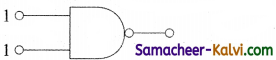
Question 46.
Which one of the following gates will have an output 1?
(a)
(b) 
(c) 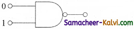
(d) 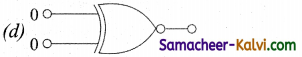
Answer:
(c)
Question 47.
If a and P are current gains in common- base and common-emitter configuration of a transistor, then p is equal to:
(a) \(\frac{1}{\alpha}\)
(b) \(\frac{\alpha}{1+\alpha}\)
(c) \(\frac{\alpha}{1-\alpha}\)
(d) α – \(\frac{1}{\alpha}\)
Answer:
(c) \(\frac{\alpha}{1-\alpha}\)
Question 48.
The truth table given below:
(a) AND gate
(b) NOR gate
(c) OR gate
(d) NAND gate
Answer:
(d) NAND gate
![]()
Question 49.
In a common base configuration of transistor \(\frac{\Delta \mathrm{I}_{\mathrm{C}}}{\Delta \mathrm{I}_{\mathrm{E}}}\) = 0.98, then current gain in common AE emitter configuration of transistor will be: [Hint: α = 0.98, β = ?]
(a) 4.9
(b) 9.8
(c) 98
(d) 49
Answer:
(b) 9.8
Question 50.
If internal resistance of cell is negligible, then current flowing through the circuit is:
For which logic gate, the given truth table is shown?
(a) \(\frac{3}{50}\)A
(b) \(\frac{5}{50}\)A
(c) \(\frac{4}{50}\)A
(d) \(\frac{2}{50}\)A
Answer:
(b) \(\frac{5}{50}\)A
Question 51.
For which logic gate, the given truth table is shown?
(a) NAND
(b) XOR
(c) NOR
(d) OR
Answer:
(a) NAND
![]()
Question 52.
In a full wave rectifier circuit is operating from 50 Hz mains, the fundamental frequency in the ripple will be:
(a) 25 Hz
(b) 50 Hz
(c) 70.7 Hz
(d) 100 Hz
Answer:
(d) 100 Hz
Question 53.
Following diagram performs the logic function of:
(a) AND gate
(b) NAND gate
(c) OR gate
(d) NOR gate
Answer:
(a) AND gate
Question 54.
Which one of the diode is reverse biased?
(a) 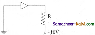
(b) 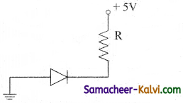
(c) 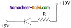
(d) 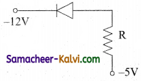
Answer:
(b)
![]()
Question 55.
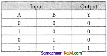
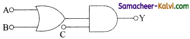
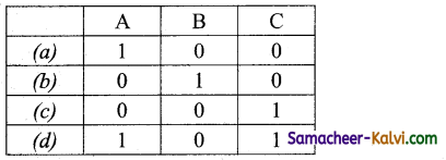
In the following circuit, the output Y for all possible inputs A and B is expressed by:
(a) Ā + B̄
(b) Ā . B̄
(c) A. B
(d) A + B
Answer:
(d) A + B
Question 56.
The output of OR gate is 1
(a) only if both inputs are 1
(b) if either or both inputs are 1
(c) if either input is zero
(d) if both inputs are zero
Answer:
(a) only if both inputs are 1
Question 57.
The peak voltage in the output of a half wave diode rectifier with sinusoidal signal without filter is 1OV. The DC component of the output voltage is:
[Hint: VDC = \(\frac{\mathrm{V}_{m}}{\pi}\)]
(a) \(\frac{10}{\sqrt{2}}\)V
(b) \(\frac{20}{\pi}\)V
(c) 10 V
(d) \(\frac{10}{\pi}\)V
Answer:
(d) \(\frac{10}{\pi}\)V
![]()
Question 58.
The circuit is equivalent to:
(a) OR gate
(p) AND gate
(c) NAND gate
(d) NOR gate
Answer:
(c) NAND gate
Question 59.
A p-n photodiode is fabricated from a semiconductor with a band gap of 2.5 eV. It can defect a signal of wavelength:
(a) 4000 nm
(b) 6000 nm
(c) 4000 Å
(d) 6000 Å
Answer:
(c) 4000 Å
![]()
Question 60.
A common emitter amplifier has a voltage gain of 50, an input impedance of 100 Ω and an output impedance of 200 Ω. The power gain of the amplifier is:
(a) 50
(b) 1250
(c) 500
(d) 1000
Answer:
(b) 1250
Question 61.
To get an inputs = 1 from the circuit shown below the input must be:
Answer:
(d)
Question 62.
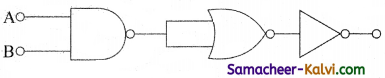
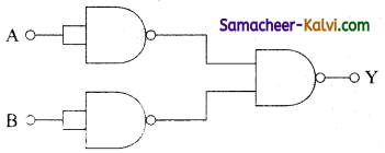
Which logic gate is represented by the following combination of logic gates?
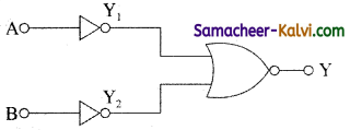
(a) NAND
(b) AND
(c) NOR
(d) OR
Answer:
(b) AND
![]()
Question 63.
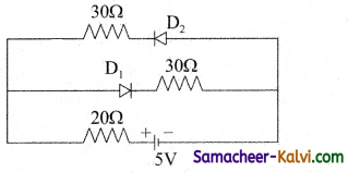
Consider an ideal junction diode, the value of current flowing through AB is:
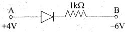
(a) 10-1A
(b) 10-3 A
(c) 10-2 A
(d) 0 A
Answer:
(c) 10-2 A
Question 64.
In the given figure, a diode D is connected to an external resistance R = 100 Ω and an emf of 3.5V. If the barrier potential developed across the diode is 0.5V, the current in the circuit will be:
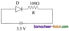
(a) 35 mA
(b) 30 mA
(c) 40 mA
(d) 20 mA
Answer:
(b) 30 mA
Question 65.
The given circuit has two ideal diodes connected as shown in figure below. The current flowing through the resistance R1 will be:
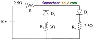
(a) 2.0 A
(b) 10.0 A
(c) 3.13 A
(d) 1.43 A
Answer:
(a) 2.0 A
![]()
Question 66.
The part of a transistor, which is heavily doped to produce a large number of majority carriers, is called:
(a) base
(b) collector
(c) emitter
(d) any one out of emitter, base and collector
Answer:
(c) emitter
Question 67.
The given combination represents the following gate:
(a) NOR
(b) XOR
(c) NAND
(d) OR
Answer:
(d) OR
Question 68.
A transistor is a / an:
(a) chip
(b) semiconductor
(c) metal
(d) insulator
Answer:
(b) semiconductor
![]()
Question 69.
Boolean algebra is essentially based on:
(a) logic
(b) numbers
(c) symbol
(d) truth
Answer:
(a) logic
Question 70.
The Boolean expression P + \(\vec{P}\) Question where P and Question are the inputs of the logic circuit, represents:
(a) AND gate
(b) NAND gate
(c) NOT gate .
(d) OR gate
Answer:
(d) OR gate
Assertions and Reasons:
In each of the following questions, a statement of assertion (A) is given followed by a corresponding statement of reason (R) just below it. Of the statements, mark the correct answer is:
(a) If both assertion and reason are true and reason is the correct explanation of assertion.
(b) If both assertion and reason are true but reason is not the correct explanation of assertion.
(c) If assertion is true but reason is false
(d) If both assertion and reason are false
(e) Assertion is false but reason is true.
![]()
Question 71.
Assertion:
A transistor amplifier in common emitter configuration has a low input impedance.
Reason:
The base to emitter region is forward biased.
Answer:
(e) Assertion is false but reason is true.
Question 72.
Assertion:
In a transistor amplifier, the output voltage is always out of phase with the input voltage.
Reason:
The emitter is more heavily doped than the other two regions.
Answer:
(d) If both assertion and reason are false
Question 73.
Assertion:
Most amplifiers use common emitter configuration circuit.
Reason:
Its input resistance is comparatively higher.
Answer:
(a) If both assertion and reason are true and reason is the correct explanation of assertion.
![]()
Question 74.
Assertion:
When the base region has larger width, the collector current increases.
Reason:
Electron – hole combination in base results in increase of base current.
Answer:
(e) Assertion is false but reason is true.
Question 75.
Assertion:
The resistivity of a semi conductor increases with temperature.
Reason:
The atoms of a semi conductor vibrate with larger amplitude at higher temperature thereby increasing in resistivity.
Answer:
(d) If both assertion and reason are false